


A leading project by: by WACKER. Category: Improving European competitiveness
Overview of the Project
WACKER launched an innovative “Etching Line Next” (ELN) project. This initiative is dedicated to developing and deploying an advanced etching process to produce hyperpure semiconductor-grade polysilicon. This material is crucial for the production of future leading-edge devices, ensuring the highest quality and yield.
The European Commission is funding the Etching-Line-Next project as part of the EU program “Important Projects of Common European Interest” (IPCEI) and the Federal Ministry for Economic Affairs and Climate Protection in Germany will also support the project together with the EU and the Free State of Bavaria.


Advancements in Polysilicon Production
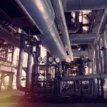
The ELN project is set to transform the production of polysilicon, a strategic raw material for microelectronics and communication technologies. The new development etching facility at WACKER’s production site in Burghausen, Germany, will produce polysilicon that meets the highest purity standards, essential for applications such as wafers for future microelectronic devices. This innovation will enhance sustainability and support the development of new technologies in the downstream value chain, including advanced sensing devices and high-frequency filter devices for 5G/6G technology.
Strategic Importance for Europe
Polysilicon is indispensable for the global electronic value chain, and Europe is in a competitive race to attract state-of-the-art semiconductor technology and investments. The ELN project will strengthen Europe’s market leadership in microelectronics, a key enabling technology for future industrial development. By producing hyperpure polysilicon locally, the project will help contribute to Europe’s technological competitiveness.
Environmental and Economic Impact
The ELN project aligns with the European Union’s Green Deal objectives by promoting climate-neutral and circular industrial production. The innovative etching process is expected to reduce raw silicon usage, decrease energy consumption and lower CO2 emissions for WACKER’s polysilicon production. Additionally, wastewater, chemical usage, and off-gas emissions will be significantly reduced, contributing to the EU’s Zero Pollution Action Plan.
Contribution to European Semiconductor Ambitions
The ELN project will play a pivotal role in achieving Europe’s semiconductor ambitions. By providing polysilicon with very low metal contamination, the company will support the development of advanced chips and innovative sensing devices. The project will also enhance the supply chain’s resilience and boost local innovation, helping Europe strengthen its presence in the microelectronic sector.
Dissemination and Community Engagement
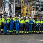
The project team recognises the importance of involving public stakeholders to foster support for the ELN initiative. The company is organising various activities, including a topping-out ceremony with community representatives, local politicians, and members of the European Commission. These efforts aim to raise awareness of the project’s significance and its positive impact on the region and Europe as a whole and to enable spillover of developments to other industries across Europe.
Follow Wacker Chemie AG
- Wacker Chemie AG on X
- Wacker Chemie AG on LinkedIn